The big picture: 2025 is shaping up to be a pivotal year for Intel’s comeback strategy. With a new CEO at the helm, the company is positioning its next-generation hardware as a litmus test for its return to the forefront of semiconductor manufacturing. As Intel’s production roadmap reaches a critical juncture, how prospective clients will respond remains uncertain.
Kevin O’Buckley, senior vice president and general manager of Intel Foundry Services, confirmed that risk production has begun for the company’s upcoming 18A semiconductor node. The announcement, made at Intel’s Vision conference, is likely to reassure investors and clients that development of the next generation of laptop and server processors has entered a crucial phase.
Risk production, an industry-standard term, refers to the stage where manufacturers refine the production process for new chips. O’Buckley explained that Intel is currently scaling up from producing hundreds of 18A wafers at a time to thousands.
Also see: How CPUs are Designed, Part 3:
Building the Chip
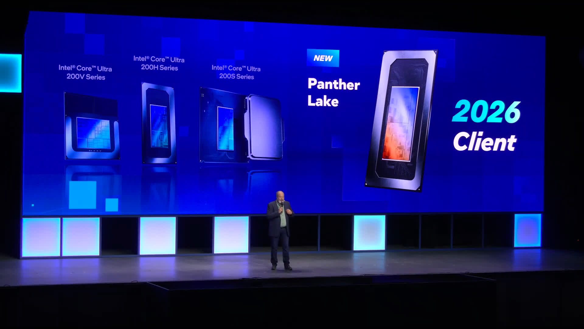
Although Intel has not yet named any external clients committed to building commercial chips on 18A, the company aims to reach volume and mass production in time to launch its Panther Lake CPUs later this year. With 28A tape-out design finalizations set to begin in the first half of 2025, Panther Lake is expected to deliver significant improvements in AI performance over Intel’s Core Ultra 200V notebook processors.
Intel’s new CEO, Lip-Bu Tan, also recently confirmed that Nova Lake and Clearwater Forest chips are scheduled for release in 2026. Nova Lake will incorporate silicon from TSMC, Intel’s foundry rival, while Clearwater Forest will bring 18A to the server market.
With 18A, Intel is racing to outpace TSMC in bringing sub-3nm technologies to market – specifically gate-all-around (GAA) transistors and backside power delivery. These innovations improve performance by reducing power leakage and enabling higher transistor density. TSMC does not plan to introduce GAA and backside power delivery until its N2 and A16 nodes debut next year. N2 is expected to enter early production soon and ramp up to mass production later this year.
Intel’s manufacturing has trailed behind TSMC and Samsung for several years. Following a string of disappointing quarters that led to the departure of former CEO Pat Gelsinger, the 18A node is seen as a crucial opportunity to reestablish confidence in Intel’s foundry business.
Nvidia and Broadcom are reportedly exploring the use of 18A for future products, though they are still in the early testing phase with Intel’s wafers. Meanwhile, Apple is expected to be the first to adopt TSMC’s N2 node, likely debuting it in the A20 processor for the iPhone 18 Pro in late 2026. AMD, Broadcom, Amazon AWS, and Intel are also expected to use N2.
Nvidia and Broadcom are reportedly interested in using 18A for future products, but the two companies are likely just running early tests with Intel’s wafers. Meanwhile, Apple is first in line for TSMC’s N2, which will likely debut with the iPhone 18 Pro’s A20 processor in late 2026. AMD, Broadcom, Amazon AWS, and Intel are also expected to employ N2.


