Forward-looking: Downscaling has long been the driving force in technological progress – from boosting computing power through smaller transistors to advancing display technology with micro-LEDs. Now, researchers from Zhejiang University and the University of Cambridge are pushing the boundaries of LED innovation even further, unveiling the world’s smallest LEDs: nano-PeLEDs, based on perovskite semiconductors.
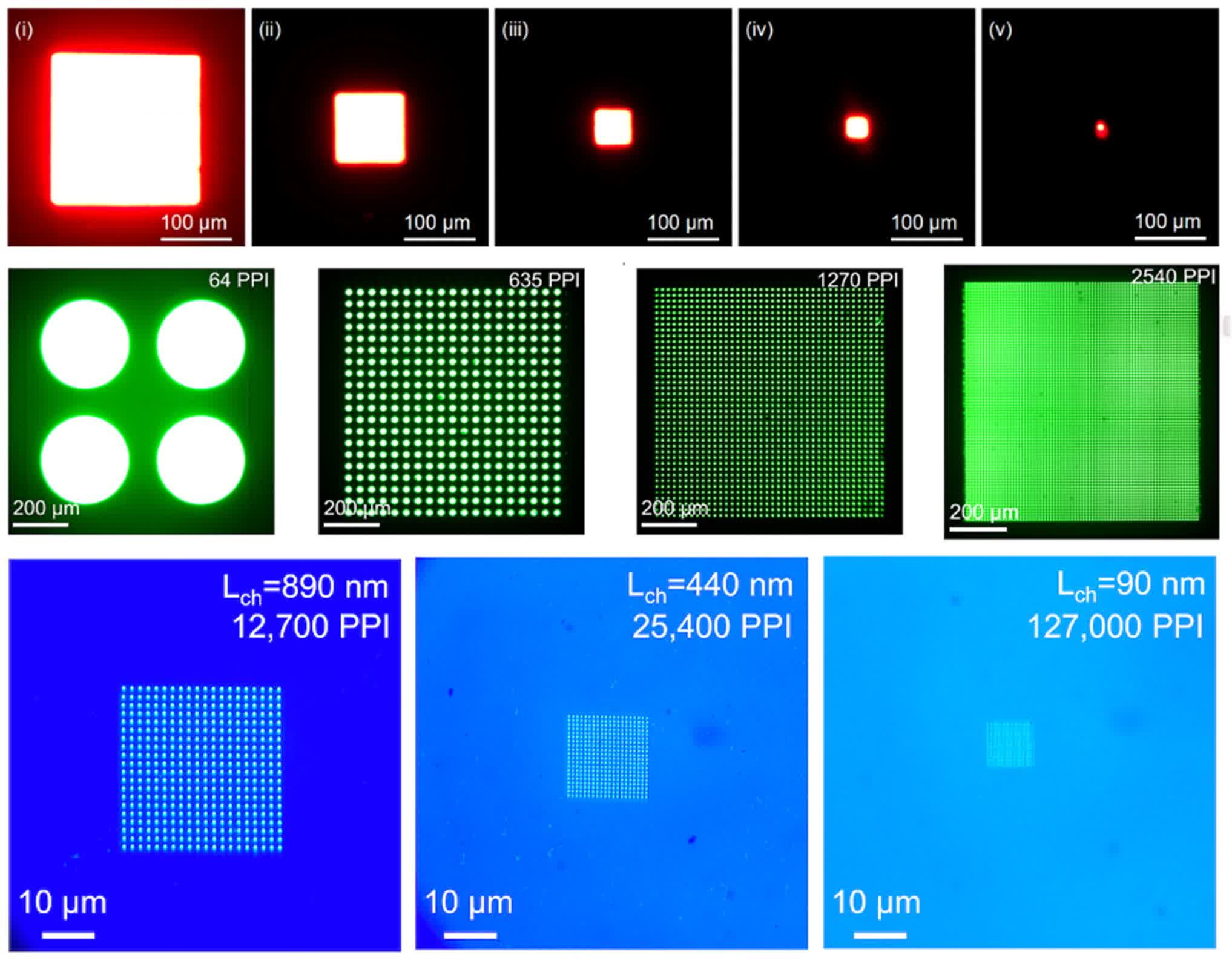
These nano-PeLEDs feature pixel lengths as small as 90 nanometers, enabling an unprecedented pixel density of 127,000 pixels per inch (PPI). For comparison, a typical 27-inch 4K gaming monitor has a pixel density of just 163 PPI.
“Making electronic devices smaller is an everlasting pursuit for scientists and engineers,” said Professor Di Dawei, Deputy Director of the International Research Center for Advanced Photonics at Zhejiang University.
He explained that while micro-LEDs based on III-V semiconductors are considered state-of-the-art, their efficiency drops sharply when pixel sizes fall below 10 micrometers – a limitation that has hindered their use in ultra-high-resolution displays.

Unlike conventional micro-LEDs, nano-PeLEDs exhibit minimal performance degradation even at microscopic scales. This resilience is attributed to their unique composition: halide perovskites – a class of semiconductors more commonly associated with solar cells. “Halide perovskites are a new class of semiconductors,” noted Professor Zhao Baodan of Zhejiang University.
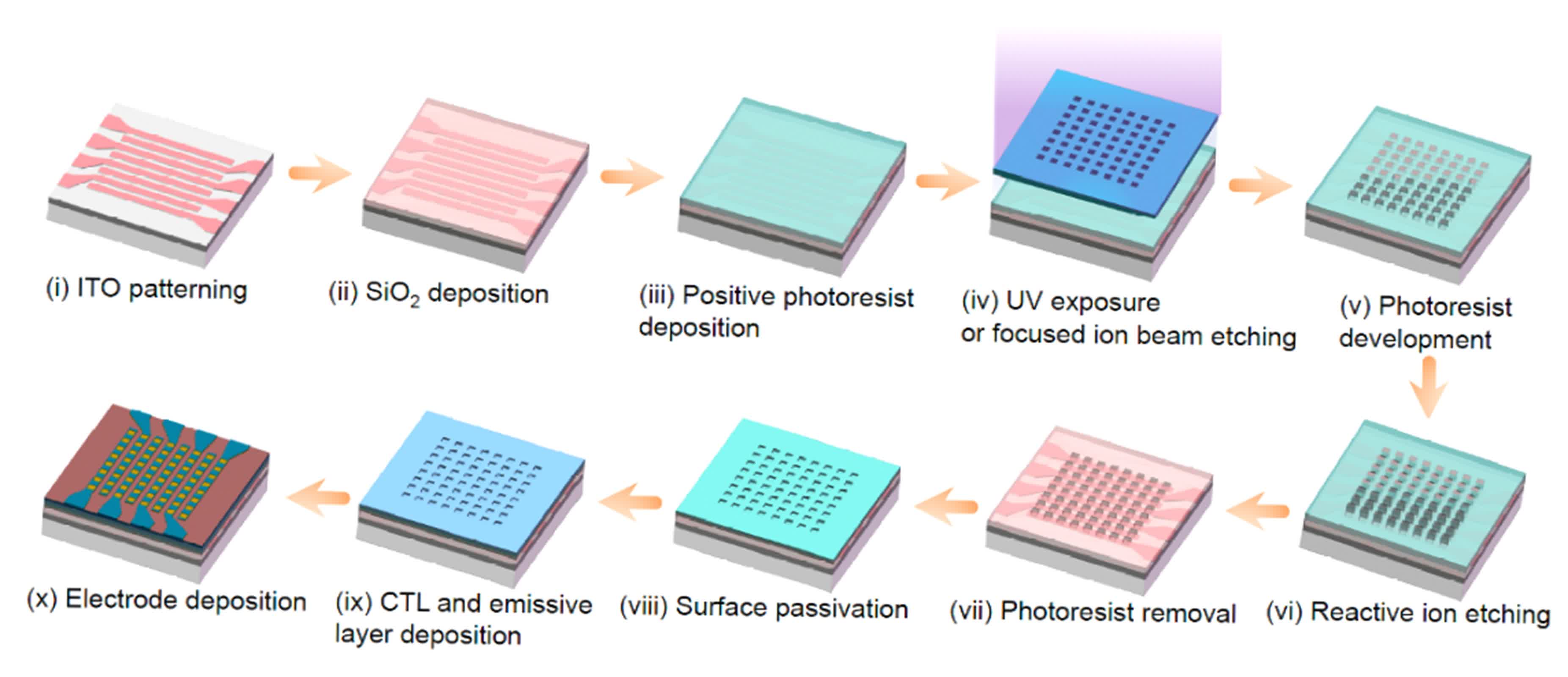
Creating nano-PeLEDs, however, was no simple task. Perovskite materials are notoriously fragile and susceptible to damage during conventional photolithographic processes used to pattern LED displays. To overcome this, the research team developed a novel fabrication method involving lithographically patterned windows in an insulating layer. This technique protects the delicate perovskite material while preserving high image quality.
“Conventional photolithographic processes are not suitable for direct patterning of the perovskite layers – it would damage the materials,” said Lian Yaxiao, first author of the study, published in Nature. “This problem is overcome by our localized contact fabrication scheme.”

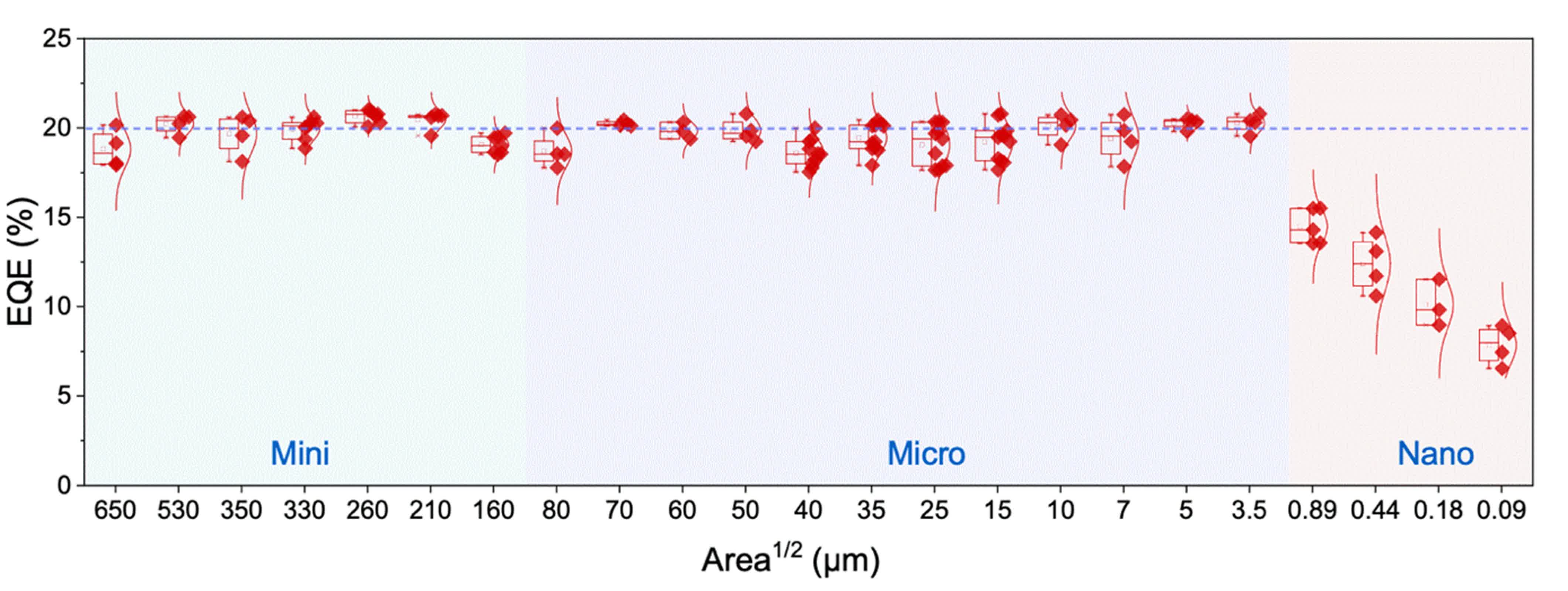
The team demonstrated that their green and near-infrared nano-PeLEDs maintained external quantum efficiencies of around 20 percent across pixel sizes ranging from several hundred microns down to just 3.5 microns.
Even at extreme miniaturization – approximately 180 nanometers – the drop in efficiency was significantly less than that seen in traditional micro-LEDs. This suggests that nano-PeLEDs could outperform III-V semiconductor-based micro-LEDs in applications requiring ultra-small pixels.

While nano-PeLEDs offer tremendous promise for high-resolution displays, practical implementation requires integration with programmable circuits capable of dynamic content delivery. To that end, Zhejiang University has partnered with LinkZill, a Hangzhou-based company specializing in thin-film transistor (TFT) technology.
Together, they developed a prototype active-matrix micro-PeLED display driven by a TFT backplane. This prototype is crucial to commercializing nano-PeLED technology and unlocking its potential for complex images and video playback.

As researchers continue refining this technology, its potential applications are rapidly expanding. The ultra-high resolution enabled by nano-PeLEDs could redefine display standards across various industries – from gaming and augmented reality to medical imaging.


